Podcast
Semiconductor Club
Hosted by Semiconductor · EN
Learn and teach anything from silicon to software online.
The Semiconductor Club is a dedicated eLearning community and marketplace for semiconductor enthusiasts. We are on a mission to bridging the gap between semiconductor domain students, professionals, institutes and companies by creating a learning ecosystem.
9episodes
Episodes
Newest firstAll episodes
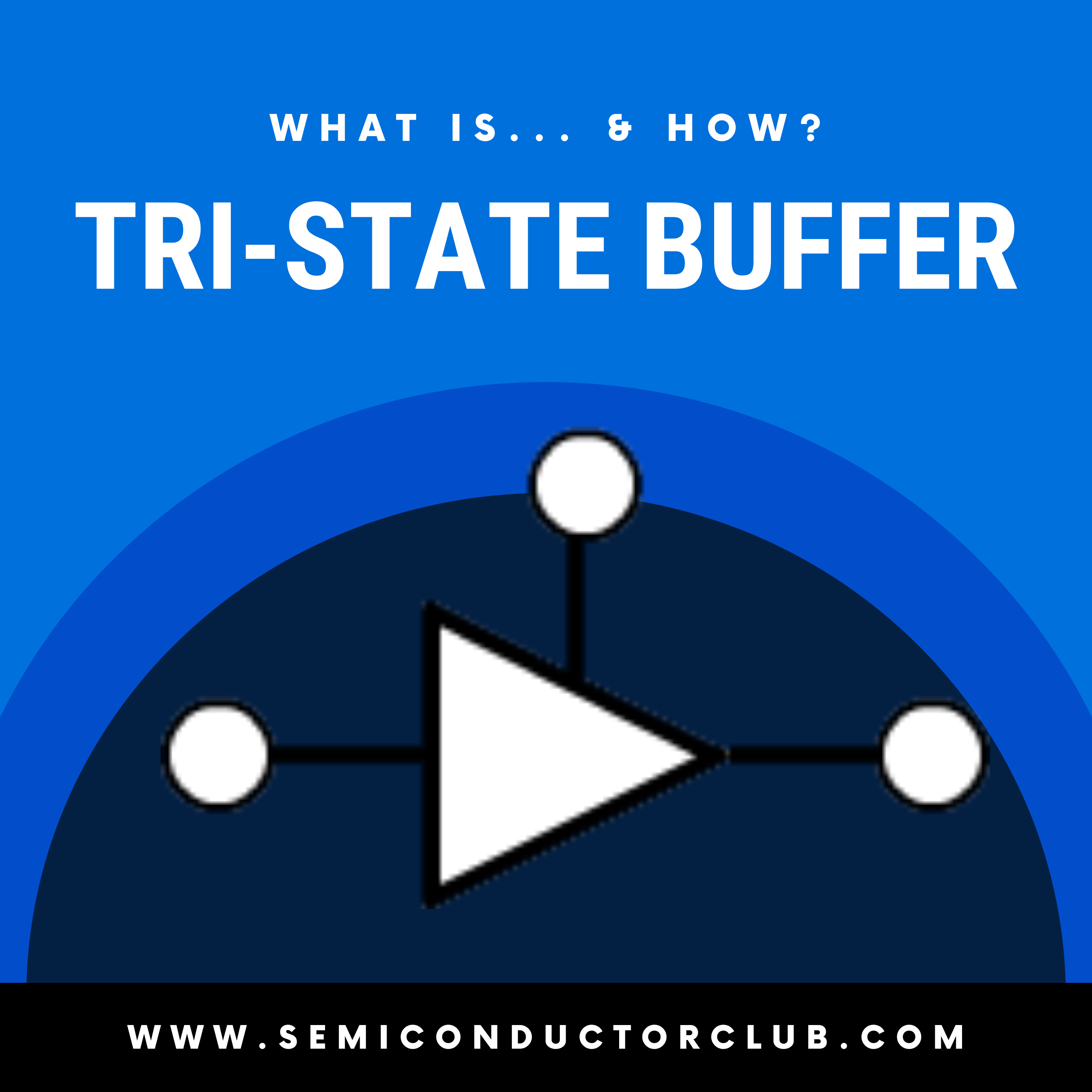
What is Tri-State Buffer & How it Works?
Nov 17, 202100:03:16Tap to summarizeLEARN & TEACH ANYTHING FROM SILICON TO SOFTWARE ONLINE: --------------------------------------------- http://semiconductorclub.com 🙋🏻♂️ SAY HI ON SOCIAL 🙋🏻♀️ --------------------------------------- YouTube: https://bit.ly/subsemicon Linkedin: https://bit.ly/lkdnsemicon Instagram: https://bit.ly/instasemicon Facebook: https://bit.ly/fbsemicon Twitter: https://bit.ly/twtsemicon
Transcribe →
What is FPGA? | Audio Article
Apr 25, 202100:05:34Tap to summarizeIn this article we will look into the basic of FPGA, the difference between ASIC and FPGA, the overview of the FPGA market, and how one can program the FPGA. So, let’s start with the basic of field-programmable gate arrays. Field Programmable Gate Arrays (FPGA) is perhaps the evolution of technology as we enter the new age. To get a brighter vision, we must first explain what a Micro Processor is. A Microprocessor is a software implemented on a silicon wafer using correct transistor connections. In other words, a simple instruction in assembly [ADD EAX, 0x04], which adds 4 to the EAX register, is no more than a command which is read by the processor ﴾the software implemented on a silicon wafer﴿ and executed after. Due to their nature, processors sequentially execute commands; you can places as many commands as you wish on storage, and ask your processor to read the storage and execute them one‐by‐one. This leads to a productive task being done, such as booting a computer or showing your operating system on your screen. READ FULL ARTICLE AT: https://semiconductorclub.com/what-is-fpga-introduction-to-fpgas/ ---x--- Join the Fastest Growing Community of Semiconductor Domain Students, Professionals, Institutes, and Companies at www.semiconductorclub.com GET YOUR FREE MEMBERSHIP NOW: ------------------------------------------------------------ http://semiconductorclub.com 🙋🏻♂️ SAY HI ON SOCIAL 🙋🏻♀️ --------------------------------------- YouTube: https://bit.ly/subsemicon Linkedin: https://bit.ly/lkdnsemicon Instagram: https://bit.ly/instasemicon Facebook: https://bit.ly/fbsemicon Twitter: https://bit.ly/twtsemicon
Transcribe →
What is High-Level Synthesis? | Audio Article
Apr 21, 202100:04:53Tap to summarizeHigh-Level Synthesis, Also known as Electronic System Level Synthesis and C Synthesis, High-Level Synthesis is an automated design procedure, that converts the algorithmic description of a system into the corresponding hardware circuit. In this process, which is actually a part of the high-level design flow, the system behaviour is described at a very high level of abstraction. This method improves productivity and reduces the chance of error. Brief History: Synopsys introduced Behavioral Compiler, the first generation behavioural synthesis tool, in 1994. Verilog was used as the input language. 10 years later, various next-generation High-Level Synthesis(HLS) tools were introduced in the market. These tools offered circuit synthesis, described in a high-level language and Register Transfer Level. Manufacturers of these tools provided extensive PC support for a wide range of tool issues. How It Is Done?: The first step in HLS is to implement the system algorithm in a high-level language, such as ANSI C, C++, System C, etc. After that, the synthesis tool generates the technical details, which is required for hardware implementation. Most of the HLS design methods use conventional logic synthesis tools by generating a Register Level Transfer (RTL) logic implementation from the system algorithm. The RTL logic is used by the traditional logic synthesis tools to generate a gate-level design. The HLS tools convert the partially timed functional code into a fully timed RTL design. The basic objective of HLS is to enable the designers to develop and test the hardware efficiently. It also gives the designers better control over the design architecture optimization. READ FULL ARTICLE: https://semiconductorclub.com/what-is-high-level-synthesis/ ---x--- Join the Fastest Growing Community of Semiconductor Domain Students, Professionals, Institutes, and Companies at www.semiconductorclub.com GET YOUR FREE MEMBERSHIP NOW: ------------------------------------------------------------ http://semiconductorclub.com 🙋🏻♂️ SAY HI ON SOCIAL 🙋🏻♀️ --------------------------------------- YouTube: https://bit.ly/subsemicon Linkedin: https://bit.ly/lkdnsemicon Instagram: https://bit.ly/instasemicon Facebook: https://bit.ly/fbsemicon Twitter: https://bit.ly/twtsemicon
Transcribe →
How to make Verilog Testbench | Audio Article
Apr 11, 202100:02:10Tap to summarizeTestBench: In Verilog is a predefined sequence of input combinations to observe the response of DUT (Design under Test). It ensures the intent of the design using different types of input vectors. Need of the Testbench: Most of the beginners observes the response of their designs by forcing the input vectors manually on the waveform window. For a newbie it is all right to start with this method, but, imagine if you are going to make some large designs means you have now more numbers of the inputs and outputs say around more than 10 then designer will not be able to test the design by simple forcing and making changes again and again. this process can take much longer time to close your design. To make the design time shorter we use some predefined sequence of the inputs which are connected to the DUT now designer have to run this testbench and observe the desired output response. This method allows debugging simpler and efficient. The DUT can be a behavioral, gate level or dataflow implementation of any design. Verilog test bench is nothing but a Verilog module. It is helpful when we need to use millions of gates on a single chip. It is also helpful while debugging and helps in debugging fast. It can be written before or after the main module but is executed only after the main module is executed. Test Bench gives designer, the liberty to use a number of inputs and observing their corresponding output in the design at the same time. Also this helps in testing the dynamic behavior of the circuit. Steps to make a Testbench: STEP 1: To create a dummy template that declares inputs to the DUT as reg and outputs from the DUT as wires. The module name in this template must be different from that of the main module. STEP 2: Connecting the DUT with testbench using Instantiation. STEP 3: Stimulation of input vectors to the DUT. STEP 4: Displaying the response of the design. Please visit “www.semiconductorclub.com/blog” to know more about all the steps in depth with example.
Transcribe →
Logic Equivalence Check | Audio Article | Semiconductor Club
Mar 29, 202100:05:55Tap to summarizeLogic Equivalence Check: ASIC design cycle involves a number of stages which varies from functional design to its verification at different levels. As soon as design is completed and verified through different methodologies is ready to go to a semiconductor chip. Hold on, it’s not simple as it said, one of the most crucial step is involved while taking RTL design to the chip level. Synthesis, which involves conversion of RTL design to the equivalent gate level netlist. This netlist is then used for the physical design implementation. Once the netlist get generated it is must to ensure that its functionality is equivalent to the RTL design from which it has been generated. The logical equivalence check performed to ensure the logical equivalency of the gate level Netlist with the RTL design. It can also be performed to check the equivalence of the: Netlist to Netlist library to library A number of EDA companies provide equivalency check tools out of them Formality (Synopsys) and Conformal (Cadence) and mostly used at industry level... READ FULL ARTICLE AT: https://semiconductorclub.com/logic-equivalence-check/ Join the Fastest Growing Community of Semiconductor Domain Students, Professionals, Institutes, and Companies at www.semiconductorclub.com GET YOUR FREE MEMBERSHIP NOW: ------------------------------------------------------------ http://semiconductorclub.com 🙋🏻♂️ SAY HI ON SOCIAL 🙋🏻♀️ --------------------------------------- YouTube: https://bit.ly/subsemicon Linkedin: https://bit.ly/lkdnsemicon Instagram: https://bit.ly/instasemicon Facebook: https://bit.ly/fbsemicon Twitter: https://bit.ly/twtsemicon
Transcribe →Logic Synthesis Steps
Mar 20, 202100:02:25Tap to summarizeArticle: Logic Synthesis is the very first step towards the physical implementation or physical design of the logic written in the form of Register transfer level(RTL). It is the process of conversion of RTL into a gate-level netlist, yes, it is the simplest definition. This conversion does not mean all to the synthesis, the most important part of the synthesis is the optimization of the netlist to make it efficient for succeeding steps. Let’s focus on the Synthesis and the steps involved in the conversion and optimization. To make things much simpler I am taking an example of a Half-adder. Step 1: Gate level model of Half adder. The inputs to the synthesis process are : Library for the standard cells as well as for macros. RTL code. Design and timing constraints. RTL of half-adder is written in the data flow modelling. Step 2: Verilog code of half adder. The code has written according to the behaviour of the logic. No hint shows how it will get implemented on the hardware or wafer. The logic synthesis tool is smart enough to make the relation of this behavioural code to the gate-level logic, so, the code will ultimately be converted into two logic gates, one is AND gate and another is XOR gate. The tool first translates the RTL to a generic gate netlist which is technology(standard cell library) independent. The tool first converts to the generic gate-level netlist so that it can perform some important logic level optimization methods like structuring and flattening which are independent of technology. Step 3 : GTECH netlist of half-adder. The generic netlist is then mapped or converted into a technology-dependent netlist, generic XOR(GTECH_xr) and generic AND(GTECH_an) is replaced by the standard cells which are present in the library. this mapping step is also involved in the optimization of the netlist to meet the Design and Timing constraints. Step 4 : Gate level netlist of half adder. Now, we have a gate-level netlist of the half adder, this netlist will be used for the physical design and other succeeding processes. Join the Fastest Growing Community of Semiconductor Domain Students, Professionals, Institutes, and Companies at www.semiconductorclub.com GET YOUR FREE MEMBERSHIP NOW: ------------------------------------------------------------ http://semiconductorclub.com 🙋🏻♂️ SAY HI ON SOCIAL 🙋🏻♀️ --------------------------------------- YouTube: https://bit.ly/subsemicon Linkedin: https://bit.ly/lkdnsemicon Instagram: https://bit.ly/instasemicon Facebook: https://bit.ly/fbsemicon Twitter: https://bit.ly/twtsemicon
Transcribe →Silicon to Software Webinar
Mar 13, 202100:39:23Tap to summarize👉🏻 Since humans are always curious to seek answers, let’s start with a few questions. Did you ever think about what actually happens inside an electronic device? Ever wonder what actually runs your mobile phone, gaming laptop, your college servers? For at least once, did you felt amazed about the ” fundamental thing” which is making all this stuff work? There is a field of study and profession which answers all these questions and pushes the world’s technology forward, calling it “the shift”. Come, explore the world of transistors a.k.a “the god particle” for the Electronics industry. Understand the world of VLSI (Very Large Scale Integration) and its future technologies. 👉🏻 Speaker: Narendra Patel – Senior ASIC Design & Verification Engineer 👉🏻 Host: Lanka Sai Charan – Member at Semiconductor Club Join the Fastest Growing Community of Semiconductor Domain Students, Professionals, Institutes, and Companies at www.semiconductorclub.com GET YOUR FREE MEMBERSHIP NOW: ------------------------------------------------------------ http://semiconductorclub.com 🙋🏻♂️ SAY HI ON SOCIAL 🙋🏻♀️ --------------------------------------- YouTube: https://bit.ly/subsemicon Linkedin: https://bit.ly/lkdnsemicon Instagram: https://bit.ly/instasemicon Facebook: https://bit.ly/fbsemicon Twitter: https://bit.ly/twtsemicon
Transcribe →Semiconductor Club (Trailer)
Mar 8, 202100:00:10Tap to summarizeNo description available
Transcribe →Semiconductor Club with Anchor.fm
Mar 8, 202100:00:10Tap to summarizeJoin the Fastest Growing Community of Semiconductor Domain Students, Professionals, Institutes, and Companies at www.semiconductorclub.com GET YOUR FREE MEMBERSHIP NOW: ------------------------------------------------------------ http://semiconductorclub.com 🙋🏻♂️ SAY HI ON SOCIAL 🙋🏻♀️ --------------------------------------- YouTube: https://bit.ly/subsemicon Linkedin: https://bit.ly/lkdnsemicon Instagram: https://bit.ly/instasemicon Facebook: https://bit.ly/fbsemicon Twitter: https://bit.ly/twtsemicon
Transcribe →